Block Diagram 741 Op Amp

Non Inverting Operational Amplifier Configuration
Lessons In Electric Circuits Volume Iii Semiconductors
The 741 Operational Amplifier
Ideal characteristics of op amp 4.
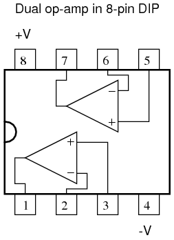
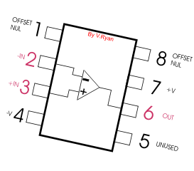
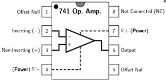
Block diagram 741 op amp. 8 pin soic pinout of ic 741 op amp and their functions the below figure illustrates the pin configurations and internal block diagram of ic 741 in 8 pin dip and to5 8 metal can package. Op amp block diagram in detail explanation. Non inverting op amp and op amp as buffer op amp as voltage follower duration. Internal block diagram of op amp 2.
Pin diagram of ic 741 op amp 3. When we on the circuit with op amp is in place initially voltage at non inverting input is higher than the voltage at inverting input and output of op amp lm741 pin 6 is high. While there are a variety of op amps each with specific inner design features such as internal frequency compensation fet inputs darlington inputs current sources as active loads input voltage and output current limiters and many others the analysis of a specific op amp equivalent circuit will provide a good basis for understanding the inner operation and construction of the op amp and. So in this article we are going to know the basics of op amp using its block diagram.
All about electronics 289444 views. We have already discussed in detail about the basics on operational amplifier its block diagram symbol different characteristics and its circuit diagram refer op amps operational amplifiersin this post we will be discussing about the 741 ic one of the most popularly used op amp ic. Block diagram of operational amplifier op amp. Block diagram of operational amplifier op amp the block diagram of a multi stage operational amplifier is given below.
The two amplifiers are applied at inverting or non inverting terminals. Some of the basic applications of an op amp are listed below. Block diagram of op amp. From the block diagram of op amp you will get sufficient knowledgeit is good to start learning everything from the basic.
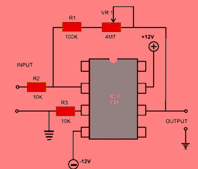
Now lets take a look at the functions of different pins of. This op amp ic comes in the following form factors. Working of the circuit is simple basically this circuit generates a square wave at the output if op amp is in working condition resulting a blinking led. 8 pin dip package.
To5 8 metal can package. In this lecture i explained the following topics.
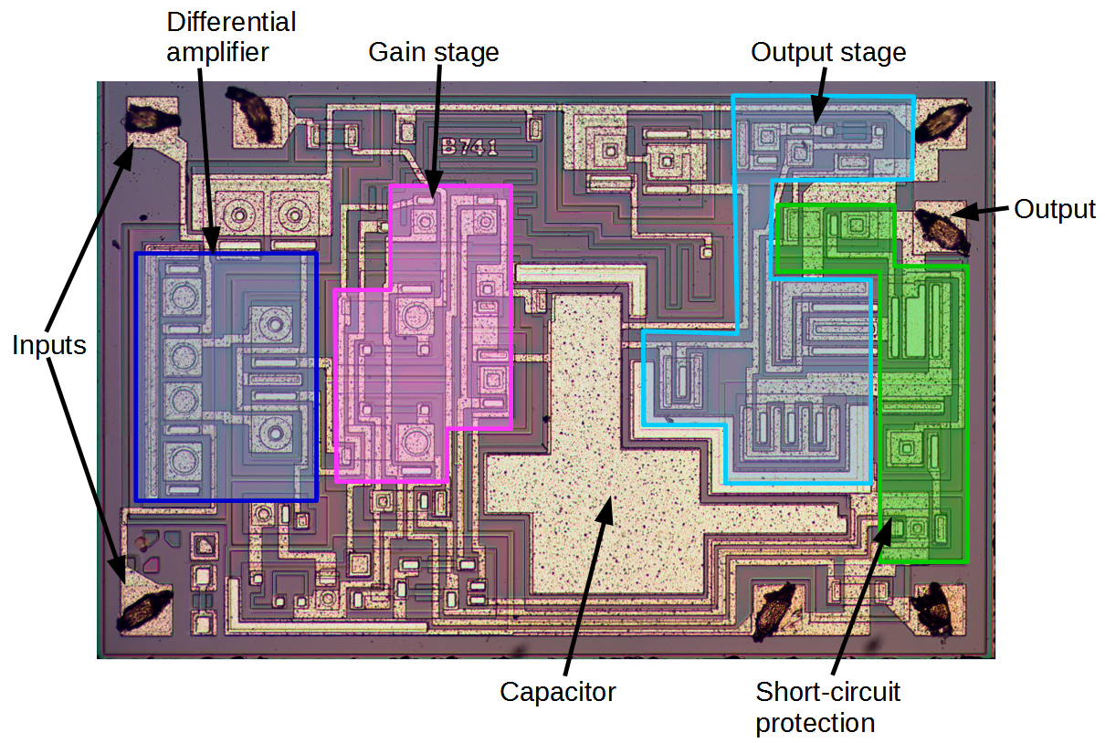
Understanding Silicon Circuits Inside The Ubiquitous 741 Op Amp
Ic 741 Op Amp Basics And Circuit Working With Characteristics

Ba 0852 Figure 1 The Opamp Ic Tester Circuit Schematic Wiring
How 741 Op Amp Power Supply Circuit Works Eleccircuit Com

Fx 6629 Op Amp 741 Ic Tester Circuit Schematic Wiring

Fv 0645 Are The Functional Blocks Of An Amplifier Free Diagram

Introduction To Operational Amplifier Characteristics Of Ideal Op

Hd 8134 Introduction To Ua 741 Opamp Electronic Circuits And Diagram
Ic 741 Op Amp Pin Configuration And Working
