Block Diagram 4 Bit Ripple Carry Adder
Virtual Lab For Computer Organisation And Architecture
4 Bit Ripple Carry Adder Using Cmos

Block Diagram Of 4 Bit Ripple Carry Adder Download Scientific Diagram
So to design a 4 bit adder circuit we start by designing the 1 bit full adder then connecting the four 1 bit full adders to get the 4 bit adder as shown in the diagram above.
Block diagram 4 bit ripple carry adder. In 4 bit adder the time delay for a valid output is the sum of time delay of 4 full adders if there is an n bit adder than the time delay will be the sum of time delay of n full adders. Image courtesy of digital design. There are a wide variety of configurations for implementing an n bit adder but to keep things simple we assume that a simple ripple carry adder is utilized. It means higher the bit size of the numbers the late the answer we will getso it is not an efficient design for complex and fast working systems.
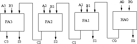
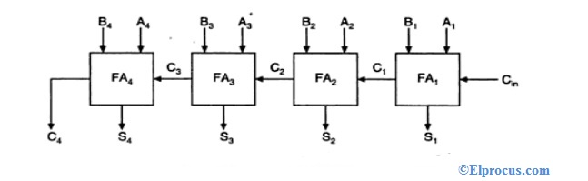
For the 1 bit full adder the design begins by drawing the truth table for the three input and the corresponding output sum and carry. Sum out s0 and carry out cout of the full adder 1 is valid only after the propagation delay of full adder 1. The block diagram of a four bit ripple carry adder. In the same way sum out s3 of the full adder 4 is valid only after the joint propagation delays of full adder 1 to full adder 4.
The main operation of ripple carry adder is it ripple the each carry output to carry input of next single bit addition. Each single bit addition is performed with full adder operation a b cin input and sum cout output. It is used to add together two binary numbers using only simple logic gatesthe figure below shows 4 full adders connected together to produce a 4 bit ripple carry adder. The main difference between the full adder and the half adder is that a full adder has three inputs.
Full adder block diagram. However the ripple carry adder is relatively slow since each full adder must wait for the carry bit to be calculated from the previous full adder. Circuit diagram of a 4 bit ripple carry adder is shown below. The same two single bit data inputs a and b as before plus an additional carry in c in input to receive the carry from a previous stage as shown in the full adder block diagram below.
A ripple carry adder is made of a number of full adders cascaded together. These block based adders include the carry skip or carry bypass adder which will determine p and g values for each block rather than each bit and the carry select adder which pre generates the sum and carry values for either possible carry input 0 or 1 to the block using multiplexers to select the appropriate result when the carry bit is known. Similarly the carry propagation delay is the time elapsed between the application of the carry in signal and the occurance of the carry out cout signal. The structure of a four bit ripple carry adder is shown in figure 2.
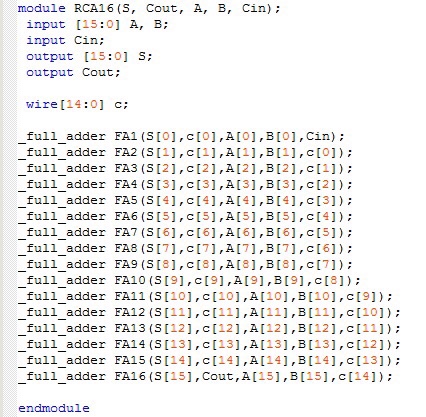
The 4 bit ripple carry adder vhdl code can be easily constructed by port mapping 4 full adder. The first and only the first full adder may be replaced by a half adderthe block diagram of 4 bit ripple carry adder is shown here below the layout of ripple carry adder is simple which allows for fast design time.
Solved Consider This 4 Bit Ripple Carry Adder Subtractor Chegg Com

2eibt9lvgnyszm
Http Ijsetr Org Wp Content Uploads 2014 05 Ijsetr Vol 3 Issue 5 1340 1345 Pdf
Ripple Carry Adder Types Workin Advantages And Its Applications
Https Escholarship Org Content Qt3dx5775c Qt3dx5775c Pdf T Pcf503

4 Bit Ripple Carry Adder Rca A 4 Bit Adder Is Implemented Using 3 Download Scientific Diagram
Structure Of Full Adder And 4 Bits Ripple Carry Adder Download Scientific Diagram

Pdf Design Of Low Power And High Speed 4 Bit Ripple Carry Adder Using Gdi Multiplexer Innovative Research Publications Academia Edu

Solved Provide The Verilog Code For A 2 Bit Ripple Carry Chegg Com
