Block Diagram Of 4 Bit Register

Fe 9043 Logic Diagram Of 3 Bit Synchronous Counter
Shift Registers Studytronics

Lessons In Electric Circuits Volume Iv Digital Chapter 12
Where m is width of address bits and n is data width.

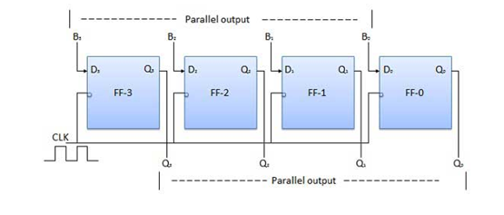
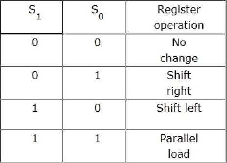
Block diagram of 4 bit register. S1s0 11 parallel data is loaded. I want to build a 4 bit shift register using d flipflop but i dont understand this diagram. There are two serial inputs namely the serial right shift data input dr and the serial left shift data input dl along with a mode select input m. S1s0 10 current state is complemented.
This block diagram consists of three d flip flops which are cascaded. S1s0 01 register is cleared to 0. You just need to have a 4 bit parallel register. Look at the di.
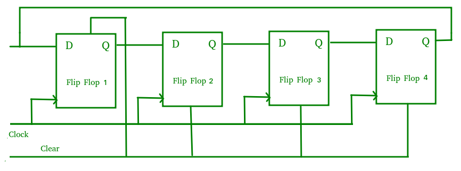
The shift register which allows serial input and produces serial output is known as serial in serial out siso shift register. A shift register basically consists of several single bit d type data latches one for each data bit either a logic 0 or a 1 connected together in a serial type daisy chain arrangement so that the output from one data latch becomes the input of the next latch and so on. A simple serial in serial out 4 bit shift register is shown above the register consists of 4 flip flops and the breakdown of how it works is explained below. This code is given to me for shift register entity shift4 is port d.
On startup the shift register is first cleared forcing the outputs of all flip flops to zero the input data is then applied to the input serially one bit at a time. A four bit bi directional shift register is shown in fig. The block diagram of 3 bit siso shift register is shown in the following figure. And 2x2 case 1.
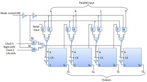
Such a register is called bi directional register. There are 3 combinations 1. Memory is mxn type. Online plc programming tutorial for shift registers using the bsr and bsl bit shift instructions duration.
Register file the interface should minimally include. A register file is a collection of kregisters a sequential logic block that can be read and written by specifying a register number that determines which register is to be accessed. An n bit input to import data for writing a write port an n bit output to export read data a read port. It is simplest case.
Below is what ive made but im not so sure if ive implemented it. This implementation is a 4 bit shift register utilising d type flip flops. A shift register serial in parallel out type consists of a group of flip flops arranged such that the output of one feeds the input of the next so that the binary numbers stored shift from one flip flop to the next controlled by a clock pulse.

What Is Shift Register Working Applications Types Of Shift
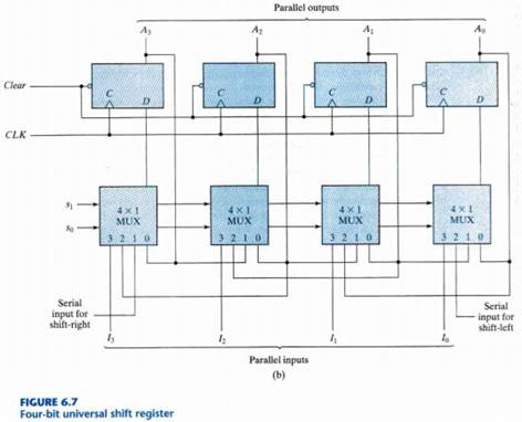
Solved The Four Bit Universal Shift Register Shown In Fig 6 7

Block Diagram Of The 4 Bit Binary Weighted Dac Download
Shift Registers In Digital Logic Geeksforgeeks
Verilog Coding Verilog Code For 4 Bit Universal Shift Register

How To Design 4 Bit Memory Using D Flip Flop Quora
Https Maxwell Ict Griffith Edu Au Yg Teaching Dns Dns Module3 P3 Pdf
4 Bit Right Shift Register
Digital Registers Tutorialspoint
