Block Diagram Of 8085 Microprocessor With Explanation
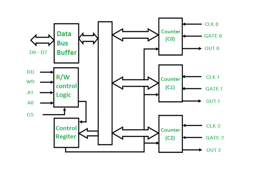
Microprocessor 8254 Programmable Interval Timer Geeksforgeeks

Intel 8085 Wikipedia
Http Ce Sharif Edu Courses 86 87 1 Ce126 Resources Root 8085 20microprocessor Pdf
They can be combined as register pairs bc de and hl.

Block diagram of 8085 microprocessor with explanation. In this article you will get to know about the definition architecture block diagram and working of 8085 microprocessor. Before knowing about the 8085 architecture in detail lets us briefly discuss about the basic features of 8085 processor. It also works as registers for io accesses. Block diagram architecture of 8085 microprocessor watch.
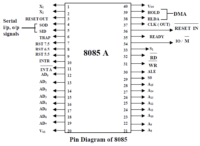
Generally the 8085 is an 8 bit microprocessor and it was launched by intel team in the year of 1976 with the help of nmos technology. As we know that a microprocessor performs arithmetic and logic operations. Pin diagram of 8085 duration. 8085 is an 8 bit microprocessor as it operates on 8 bits at a time and is designed with n mos technology.
The address and data bus are multiplexed in this processor which helps in providing more control signals. The six general purpose registers are used to store 8 bit data. The configurations of 8085 microprocessor mainly include data bus 8 bit address bus 16 bit program counter 16 bit stack pointer 16 bit registers 8 bit 5v voltage supply and works at 32 mhz. Acumulator it is a 8 bit register which is used to perform airthmetical and logical operation.
And an 8086 microprocessor is able to perform these operations with 16 bit data in one cycle. It uses a single 5v supply for its operations. Features of 8085 microprocessor. 8085 microprocessor has 1 non maskable interrupt.
It stores the output of any operation. A15 a8 it carries the most significant 8 bits of memoryio address. Its clock speed is about 3mhz. It is 8 bit mp.
This is the function al block diagram of 8085 microprocessor. Control and status signals. 8085 microprocessor is an 8 bit microprocessor with a 40 pin dual in line package. It is a 40 pin dual in line chip.
Block diagram of 8085 microprocessor with detailed explanation. Functional block diagram of 8085 microprocessor. Introduction to 8085 introduced in 1977. Architecture of 8085 microprocessor with block diagram 8085 microprocessor microprocessor duration.
This is the functional block diagram of the 8085 microprocessor. The following image depicts the pin diagram of 8085 microprocessor the pins of a 8085 microprocessor can be classified into seven groups address bus. This processor is the updated version of the microprocessor.
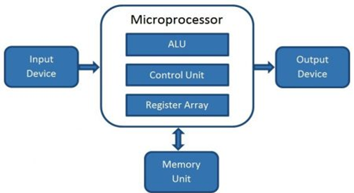
What Is Microprocessor Block Diagram Evolution Working
8085 Microprocessor Study Notes For Electronics And Communication
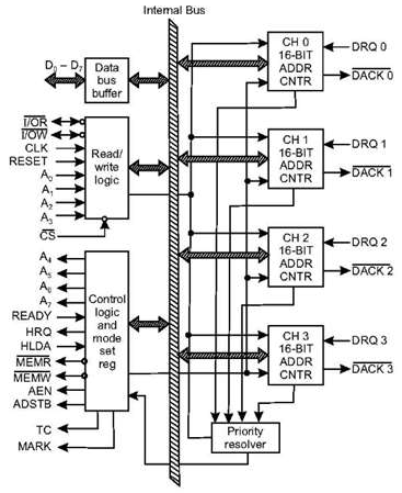
Microprocessor 8257 Dma Controller Tutorialspoint
8259 Pic Microprocessor Geeksforgeeks
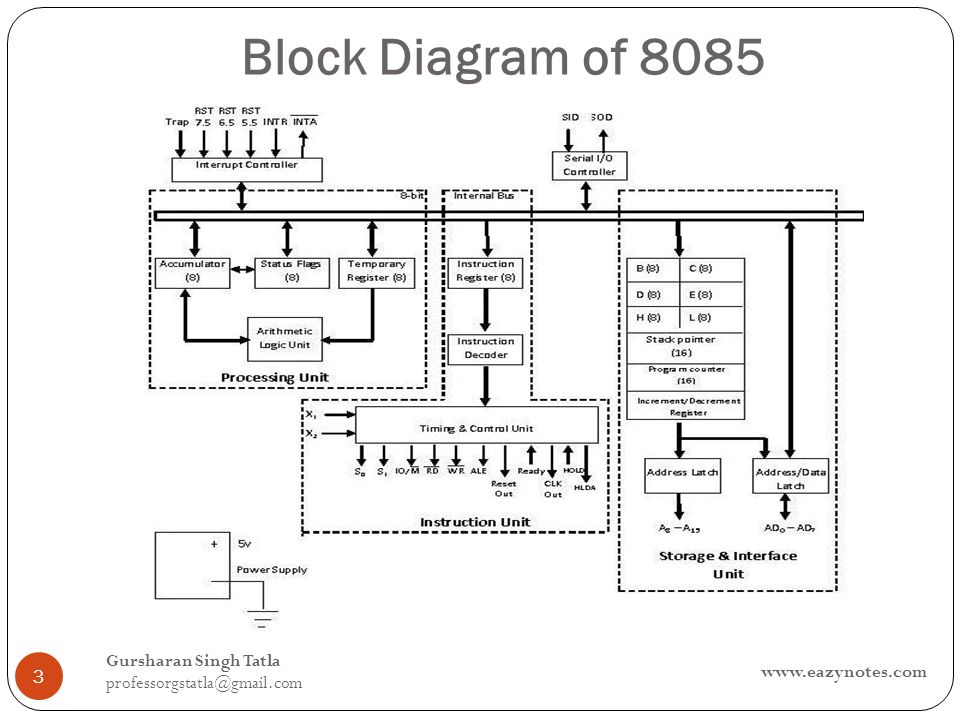
Block Diagram Of Intel 8085 Gursharan Singh Tatla Ppt Download

Kd 1634 Assembly Program To Interface Traffic Light Controller
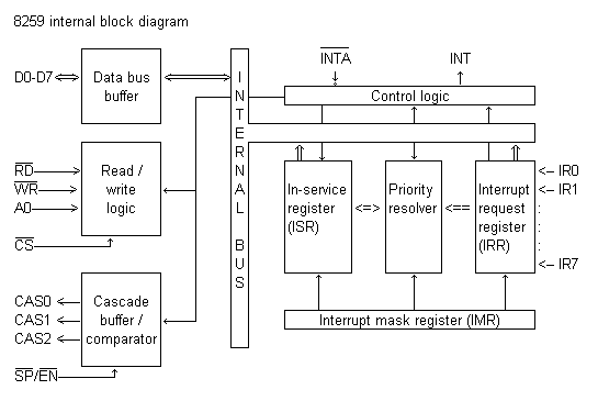
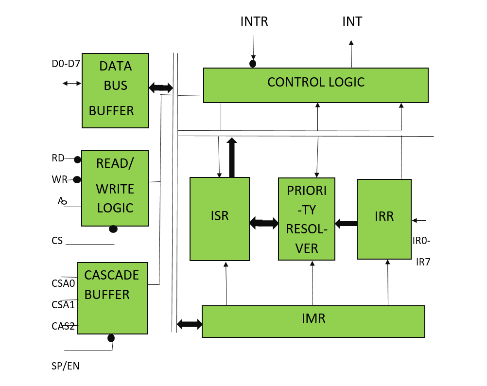
8259 Programmable Interrupt Controller
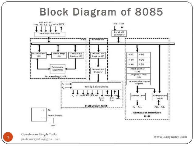
Block Diagram Of 8085
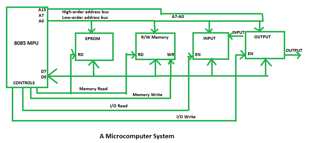
Introduction Of Microcomputer System Geeksforgeeks
