Logic Diagram Truth Table

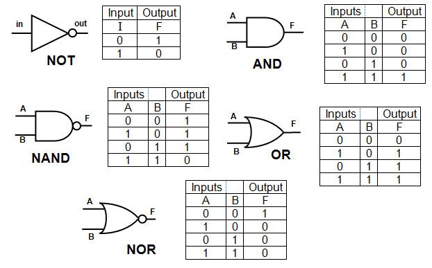
Logic Gates Logic Gate Symbols Logic Diagram Truth Table
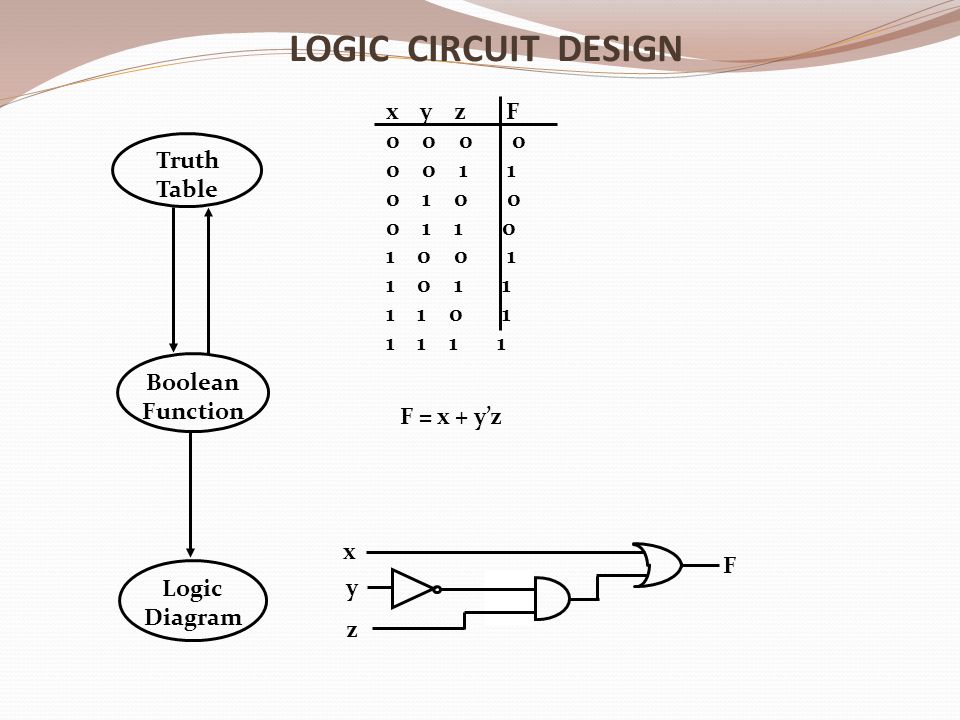
Part 2 Design Circuit Logic Circuit Design X Y Z F F X Y Z
Schoolphysics Welcome
Download the notes topic 1.
Logic diagram truth table. Truth table karnaugh map minimal form gate diagram. Boolean expression we will discuss each herein and demonstrate ways to convert between them. Binary to bcd code code converter. From the above truth table the boolean equation for the output is given as.
In many computers and other types of processors adders are used to calculate addresses similar operations and table indices in the alu and also in other parts of the processors. The full adder fa circuit has three inputs. Truth table karnaugh map minimal form gate diagram duration. An adder is a digital logic circuit in electronics that performs the operation of additions of two number.
Truth table to determine if an. A truth table is a mathematical table used in logicspecifically in connection with boolean algebra boolean functions and propositional calculuswhich sets out the functional values of logical expressions on each of their functional arguments that is for each combination of values taken by their logical variables enderton 2001in particular truth tables can be used to show whether. Titlefull adder truth table logic diagram class. The inputs are represented by x y and z while the compliments are.
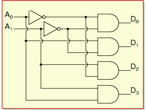
Logic representation there are three common ways in which to represent logic. 3 to 8 line decoder has a memory of 8 stages. From this truth table the k maps are drawing shown in figure 1 to obtain a minimized expression for each output. Determing the truth table and logic statement anna does some physics.
Sr flip flop is the simplest type of flip flops. Sr flip flop construction logic circuit diagram logic symbol truth table characteristic equation excitation table are discussed. You can clearly see the logic diagram is developed using the and gates and the not gates. Half adder and full adder.
Drawing of k map for each output. Adders are classified into two types. Logic circuit diagram 3. Explain half adder and full adder with truth table an adder is a digital logic circuit in electronics that implements addition of numbers.
Steven petryk 138158 views. From the above boolean equation the logic circuit diagram of an 8 to 1 multiplexer can be implemented by using 8 and gates 1 or gate and 7 not gates as shown in below figure.

T Flip Flop Logic Diagram And Truth Table

Encoders And Decoders Types And Its Applications

Logic Design Using Stateflow Truth Tables Matlab Simulink

Logic Or Gate Tutorial With Logic Or Gate Truth Table

Logic Diagram And Truth Table Wiring Diagram
Logic And Boolean Expressions

Gx 4557 Logic Diagram For D Flip Flop Wiring Diagram

Pin On Electronics

Logic Diagram And Truth Table For Negation Download Scientific
